PCB Via Size and Pad Size Guidelines, Zach Peterson
By A Mystery Man Writer
Description
Do you know what PCB via size you should use in your PCB layout? We’ll look at a few simple ways to answer this question.

BGA Pad Size Deep Dive Component Creation

Oxford Splash Pad Construction Expected to Start in April
The SuperCam Instrument Suite on the NASA Mars 2020 Rover: Body Unit and Combined System Tests

US9465412B2 - Input device layers and nesting - Google Patents

Stitching Via Deep Dive

Design007 Magazine :: I-Connect007

Charles Pfeil on LinkedIn: #electronics #pcbdesign #highspeed #pcb #mentor #cadence #design #digital

3210 PDFs Review articles in PCB DESIGN
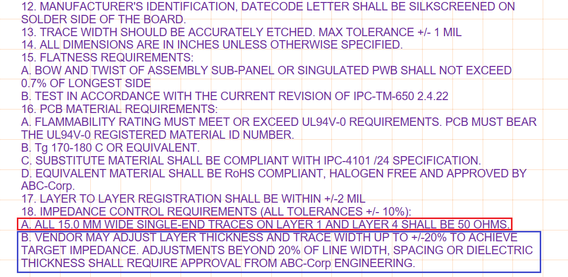
Communicating PCB Layer Stackup Needs to Manufacturers, Zach Peterson, PCB Design Blog

PCB Via Size and Pad Size Guidelines, Zach Peterson, Blog

A cell-type-specific atlas of the inner ear transcriptional response to acoustic trauma - ScienceDirect

Review request - ESP32 WROOM module based RS232 controller : r/PrintedCircuitBoard
from
per adult (price varies by group size)